WP4
- Home
- »
- WP4

Electron optics and detectors
The current imaging tools in TEM face challenges like low speed, imprecise beam shaping and limited data storage, impacting the imaging process significantly. Low speed limits the study of rapid processes, imprecise beam shaping affects results clarity, and limited data storage restricts indepth analysis. Addressing these challenges is crucial for advancing electron imaging capabilities and gaining more comprehensive insights into the nanoscale world.
The aim of WP4 is to drive advancements in electron imaging and spectroscopy tools by developing new detectors and optics with enhanced capabilities. This endeavor involves addressing various challenges, such as refining time resolution, shaping electron beams, optimizing data storage and enabling high-speed measurements for a profound understanding of electron behavior.
OBJECTIVE 1
To develop a device for the detection of electron-related events
This objective seeks to improve electron detection by introducing a smart solution for efficiently managing data from complex experiments. This includes an adaptable triggering system and a rapid data processing method.
The adaptable triggering system helps initiate and control experiments, while the rapid data processing method ensures quick and efficient analysis of the collected data. The practicality and benefits of recording comprehensive event details during experiments will be evaluated.
The goal is to explore applications in automated user-oriented methods for a more accessible and efficient research platform.

OBJECTIVE 2
To explore methods for electron beam optimization in life science imaging
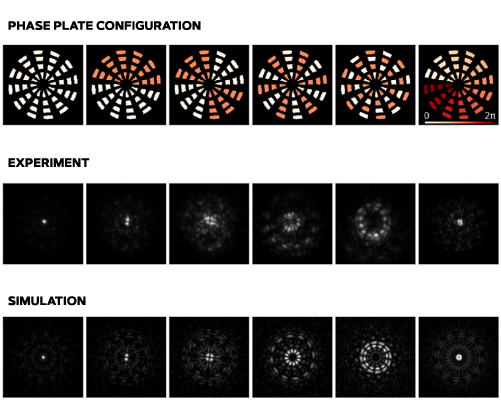
This objective aims to make electron imaging in the life sciences more efficient by minimizing beam damage and improving image clarity. This involves using specialized electrostatic phase plates and advanced data processing techniques to control electron beams precisely. The aim is to enhance image quality by optimizing electron flux, reducing damage and improving interpretability.
The goal is to establish user-friendly workflows and explore innovative laser-driven methods for shaping electron beams at high speeds.
OBJECTIVE 3
To develop advanced spectroscopy techniques for semiconductors
In semiconductors, the generation and transport of electrons that have moved to a higher energy state (excitation) are pivotal for various technological applications, including light-emitting diodes, solar cells and quantum information processing. Analysing these processes typically involves optical techniques like photoluminescence (PL) and electron microscopy coupled with spectroscopy methods such as electron energy loss spectroscopy (EELS) and cathodoluminescence (CL).
Recently, a technique called cathodoluminescence excitation spectroscopy (CLE) has emerged, linking electron energy absorption (EELS) to photon emission (CL) for measuring semiconductor quantum efficiency. This technique has the benefit of measuring the rise and decay times of excitations created in materials.
The aim of this objective is to enhance the temporal resolution of CLE to below 1 nanosecond and extend the accessible temperature range for sample analysis down to below 70 kelvin, facilitating the study of technologically relevant semiconductor materials.

“Our goal is to lead the development of new electron phase shaping and event based detection for advanced imaging and spectroscopy and to make these disruptive technological innovations accessible to diverse user communities.”
Luiz Galvão Tizei
WP4 Team Leader
